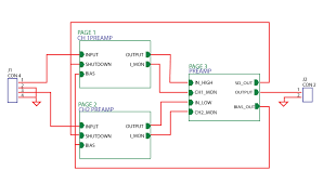
A PCB schematic diagram is a drawing that describes the structure of a PCB. The process of creating a PCB schematic diagram begins by finding the core components of a functional unit. Once the core components are identified, the next step is to connect the traces between them. This is called the functional partitioning. It can be easier to partition a PCB schematic diagram if you know the serial numbers of the components.
Reverse-engineering a PCB
A PCB schematic diagram is a convenient way to document an integrated circuit’s electronic circuitry. It consists of different symbols that represent the different types of electronic components. If a customer requests a schematic diagram, the engineers at Fast PCB Studio reverse-engineer it for them based on the PCB module. This diagram is then provided to the customer for future reference. Reverse engineering is an important tool in the integrated circuit industry.
First, it is important to make a sketch or photograph of the PCB. Make sure the image has two sides and is on a dark background. This will prevent any confusion about the structure of the PCB.
Creating a PCB schematic
There are several essential elements to include in a PCB schematic diagram. First, the schematic must include all part values, manufacturing information, net names, and other pertinent information. It should also have a revision history so that any changes made in the schematic are documented. Another important feature of a schematic is a table of contents, which lists all the topics that are included in the schematic. Using this feature can make your schematic layout easier to understand and more precise.
PCB schematic diagrams are the basis of your designs, so they should include all circuit paths and descriptions of all components. You can import schematics from an EDA application into PCB editing software. Be sure to follow all component placement and footprint specifications.
Using a pcb schematic to design a PCB
When designing a PCB, a schematic diagram is a handy tool. It allows you to quickly and easily see any errors in your design. It also has a handy feature of automatically checking your design for errors. The first step is to open up a new project in your PCB design software. From the File menu, select New -> Schematic.
A schematic shows all of the connections of the circuit in a simplified way. However, this does not mean that all connections are connected in the same way. The circuit design may have connections that are very close to one another or on opposite sides.


